Overview
An IRLabs client using our IREM-IV photon emission microscope at several of their chip fabs contacted us about automating probing and data acquisition for fault analysis of a wafer. Their current practice was to assign one engineer to manually probe each test site to detect any emission irregularities and defects, which was very labor intensive.
After meeting with our client and understanding their requirements, we were able to complement our expertise in IR emission microscopy and fault analysis applications with lab automation and machine vision to design an automated wafer prober that can test and report in hours instead of days. The client saves significant time in testing and, by retrofitting their existing system with automated wafer probing, did not incur the capital expense of purchasing an entirely new system to meet their goals.
See the Wafer Prober in Action
Key Facts
Project: Automated Wafer Prober for Design Fault Analysis
Project Location: Multiple international locations
Application: Semiconductor Fault Analysis
IRLabs’ Product: Automated Wafer Prober
Customer Challenges & Testing Requirements
Manual probing and testing require an engineer to move the wafer so the test site is the correct position for the MCT camera, align the probe pins to precisely to the target electrical contacts, make the electrical contact, acquire the image data, then prepare to move to the next test site. Manual probing and data acquisition of a wafer was too labor intensive, taking an engineer about one week (~40 hours) to complete testing of one wafer with 300 to 400 devices and multiple test sites per device.
In addition to reducing time through automation, our client also required two types of probing: one using a custom probe card for automated testing and the other using individual probe pins to retain manual function if desired. Both probing systems were to use the same data acquisition and reporting software.
Technical challenges included correction for wafer curvature and accessing both the top and bottom surfaces of the wafer during probing and imaging functions. The MCT camera operates very close to the bottom surface of the wafer while the probe pins and alignment processes operate on the top surface of the wafer, but wafers are not completely flat. They can have a minute bow towards the middle which changes where the MCT camera focuses from underneath the wafer and can change the distance from the pin to the test site to make precise electrical contact with the top surface of the wafer. Testing operations need to access both sides of the wafer.
The IRLabs Solution
We worked with our client to develop a system to perform to their requirements in three key areas: customizable set up and programming, autonomous operation, and probe card and manual pin probe capabilities.
Customizable Set Up and Programming
We developed a programmable wafer stage and probe stage for efficient and accurate testing of the full wafer. Operators can program the wafer stage X and Y axes and the prober Z axis. Using our AIRIS Wafer Stage and Wafer Navigation software, an operator can upload a file that defines the wafer parameters and all test locations for mechanical alignment of the wafer. After alignment, the operator writes a script (software snippet) to instruct the system where to test, images to collect, and set integration time. After initial setup, the wafer prober operates automatically to test the full wafer. Setup parameters and scripts are stored for easy selection to repeat an entire automation routine.
Autonomous Operations with Accurate Autofocus Routine
After initial alignment with the pre-programmed wafer stage and probe stage, the operator initiates autonomous operation. The probe card activates each test site on the wafer automatically, accurately, and quickly. We added a new alignment microscope for ease and accuracy to the initial setup and fine alignment. A newly developed autofocus software routine automatically corrects for any wafer curvature by autofocusing the MCT camera, feeding this position to the wafer controller, and automatically adjusting for the distance of the pin movement required. The autofocus routine ensures the wafer prober applies the correct pressure to each electrical contact to produce reliable product data collection and crisp, in-focus emission images.
Access to the top and bottom of the wafer was achieved with a carbon fiber holding fixture.
Probe Pin Card and Individual Probe Pin Options
Depending on their testing needs, the Automated Wafer Prober can be operated either with a custom probe card or individual probe pins.
Our client uses custom probe cards. Probe cards can vary in form factor, so we designed the probe card mounting fixture to accommodate variations. Once mounted, the probe card performs the programmed, repeatable testing quickly with automation and accurately with autofocus.
If manual testing is desired, individual probe pins can be mounted using micromanipulator stages for precise manual alignment and control. From the workstation, the operator uses a joystick to control navigation on the X, Y and Z axes to precisely position each pin and activate the test site. Once aligned the individual probes can be raised and lowered using the probe stage interface within AIRIS.
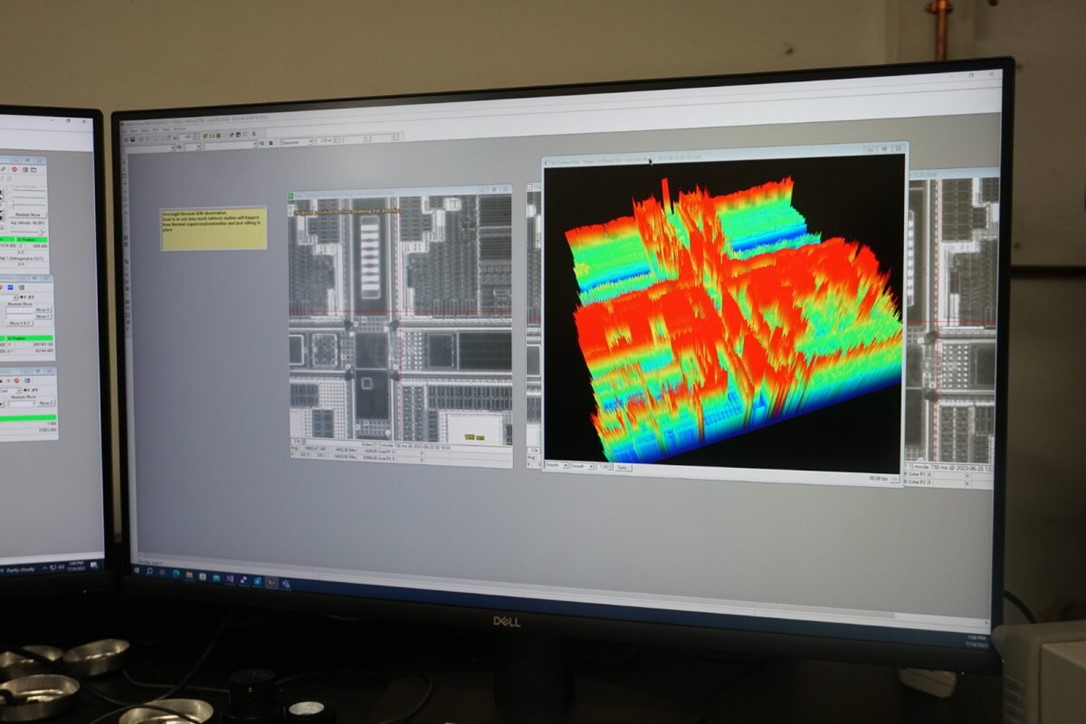
IR emission data from the MCT camera

Individual pin probe set up for manual testing

Individual pin probes can be operated manually
Data Acquisition and Reporting
Data acquisition at each test site is completely customizable for the operator using the AIRIS scripting language. At each site, users can configure their test script to switch to different lenses, change filters, change camera acquisition settings, and run external programs to control test equipment. The Wafer Automation interface also contains a GUI that shows which sites were tested, and which sites completed testing successfully. Test reports can also be generated within the AIRIS scripting language.
The outcome has been very successful for our client. After initial set up and alignment, automation enables our client to typically complete testing in less than one minute per device, including the time needed to move from one device to the next, autofocus, land the electrical contacts, collect and save image data. Before automation, testing was up to 10 minutes per device .
By working collaboratively with our client, we were able to design a solution to meet their objectives.
 Mounted DT670 Temperature Sensor
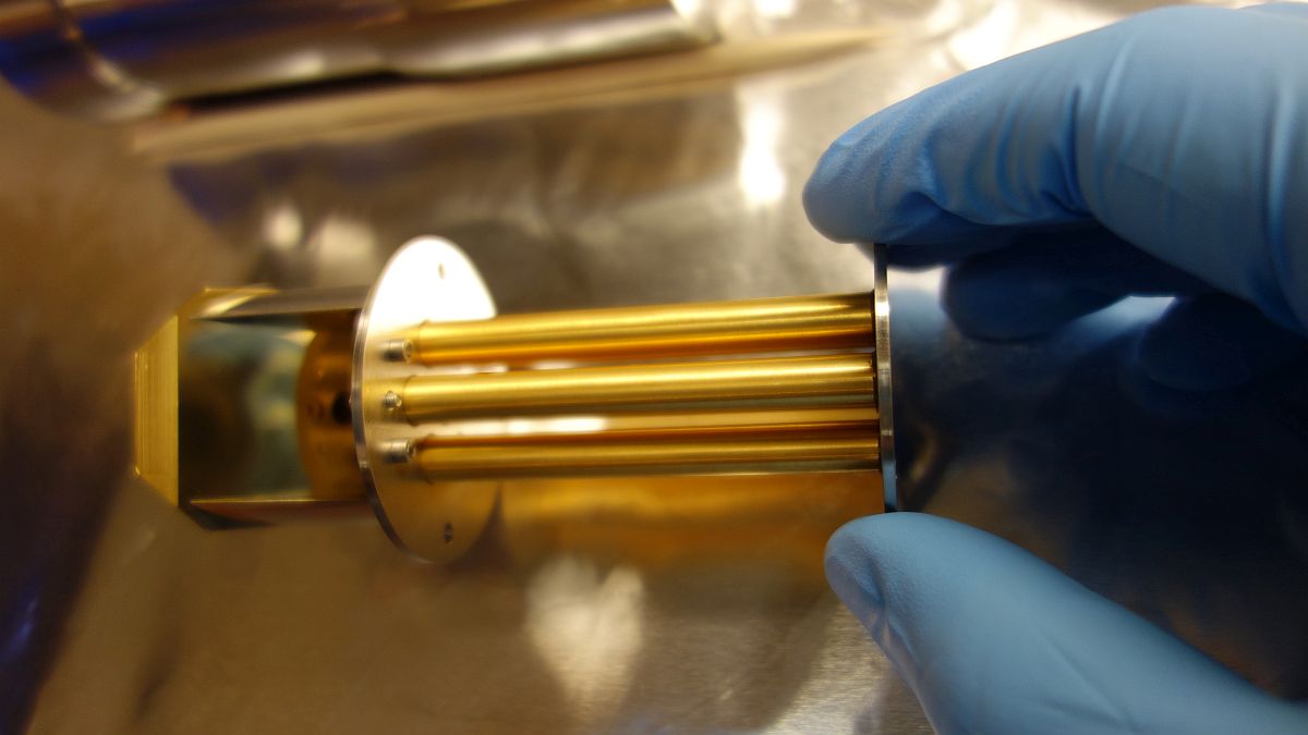
  Standard Cylindrical Getter
  Rigel Dewar
  Heater Button
 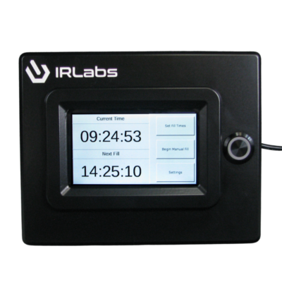 Autofill Controller