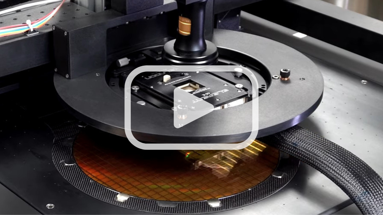
IREM-IV users can add automated electronic contact testing of full wafers to the IREM-IV to identify defects and errors with the highest reliability. The Automated Wafer Prober can accept either a custom probe card or individual probe pins and is easily programmed to collect emission data from a full wafer and store the data for analysis.
Automated for Repeatable, Faster Testing
After initial alignment, the Automated Wafer Prober will activate each test site on a wafer automatically, accurately, and quickly. Setup parameters are stored for ongoing and future testing and analysis. A new alignment microscope adds ease and accuracy to the initial setup and fine alignment.
Programmable Wafer Stage and Pin Stage
Using AIRIS Wafer Stage and Wafer Navigation software, users can program the wafer stage XY axes and the prober Z axis. After initial setup, the wafer prober will operate automatically to test the full wafer in a fraction of the time of manual probing.
IR Camera with Autofocus Enables Correct Probe Pressure
The Automated Wafer Prober operates with data from the autofocus feature of AIRIS control software. Data from autofocus allows the wafer prober to apply the correct pressure to each electrical contact, ensuring reliable product data collection and crisp in-focus emission images.
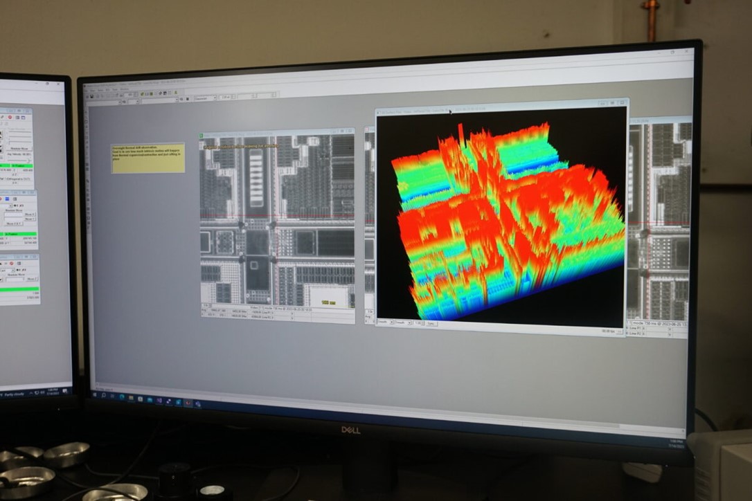
The photon emission microscope and MCT camera images IR emission data.
Probe Pin Card or Individual Probe Pins
Depending on the testing needs, the Automated Wafer Prober can be operated either with a probe card or individual probe pins. Individual probe pins can be mounted using micromanipulator stages for precise alignment and control.
Features:
● Automated alignment and operation for faster, repeatable testing
● Custom probe card or individual probe pin options
● Test wafers up to 300mm in diameter
● Automatically corrects for wafer curvature
● Retrofit available for installed IREM systems
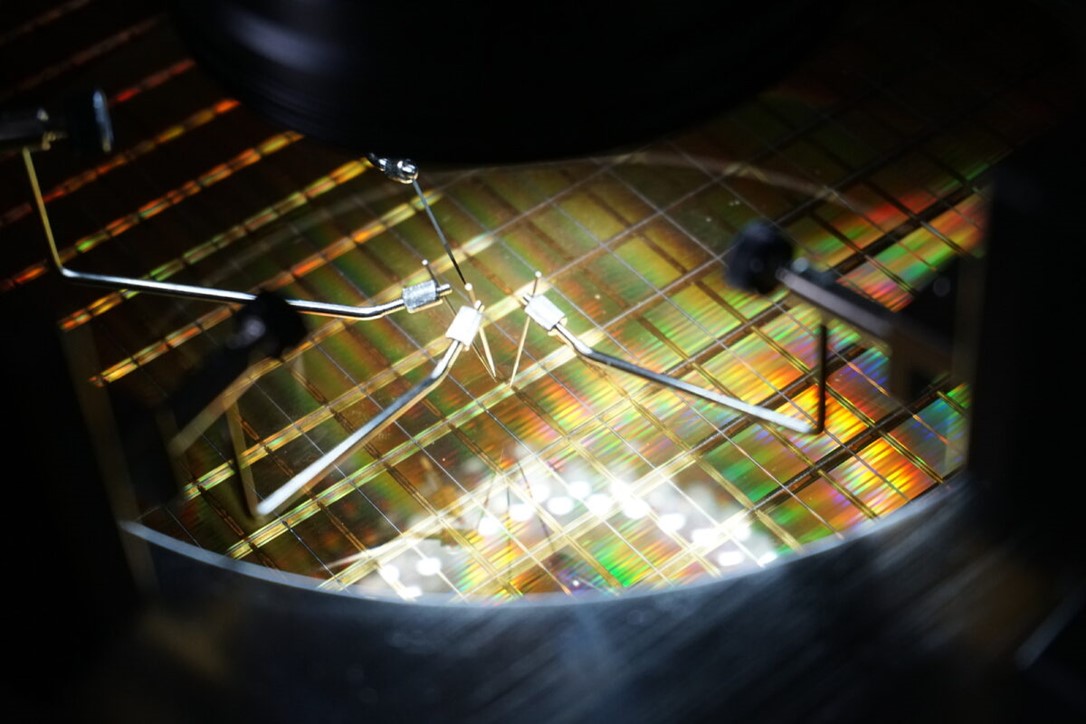
Individual probe pins can be operated manually.